充电泵是一种利用电容和高速开关来实现的简单DC-DC变换器,一般用于低电流低成本的场景中。比如在OLED的驱动芯片中,都会集成充电泵电路来为显示屏提供较高的电压。各大芯片厂商都有对应的芯片方案。
下面这个图能够有助于理解充电泵的工作原理:
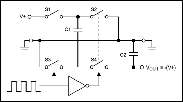
上图可以实现由正电源(比如+5V)向负电源(-5V)的转换。
Closing S1 and S3 charges the flying capacitor, C1, to V+ in the first half cycle. In the second half, S1 and S3 open and S2 and S4 close. This action connects the positive terminal of C1 to ground and connects the negative terminal to VOUT. C1 is then in parallel with the reservoir capacitor C2. If the voltage across C2 is smaller than that across C1, charge flows from C1 to C2 until the voltage across C2 reaches -(V+).
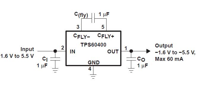
TI(德州仪器)有一款芯片型号是TPS6040x,就是实现了反向电源转换器的功能,电路非常简单,只需要额外三个电容即可。
这个芯片用的比较广泛,然后国内厂商就开始仿制了,国内有一款型号是SGM3207的芯片,可以完全兼容TPS60401,而且Datasheet的文字都很相似。当然,国产的价格是有一定优势的。
我做了一片小的实验板,实践了一下。

左端输入+5V电源,右端即可输出+5V和-5V两路电压。这种电路的问题是驱动能力比较弱,负载稍高,输出电压就会大幅度跌落,所以只适合轻微负载的应用。
原理图非常简单,参考Datasheet即可,这里就不放了。
参考资料:
https://www.maximintegrated.com/en/app-notes/index.mvp/id/725
http://cn.sg-micro.com/index.php?m=default.products_show&title=SGM3207
http://www.ti.com/product/tps60401
